INFORMATION
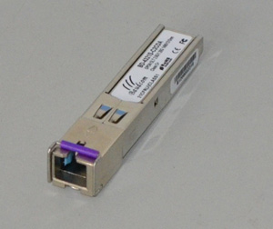
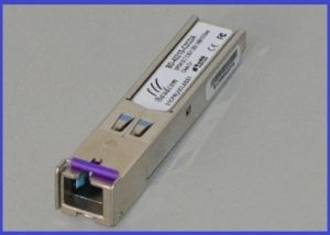
GPON OLT C+++
Features
u Single fiber bi-directional
data links asymmetric TX 2500Mbps/RX1250Mbps application
u 1490nm continuous-mode DFB
laser transmitter and 1310nm burst-mode APD-TIA receiver
u Small Form Factor Pluggable
package with SC/UPC Connector
u Single 3.3V power supply
u Digital diagnostic
monitoring interface
u Low EMI and excellent ESD
protection
u RoHS6 Compliance
u LVPECL compatible data
input/output interface
u Class I laser safety
standard IEC-60825 compliant
u LVTTL fast receiver Signal
Detect (SD) indication response
u LVTTL transmitter disable
control and transmitter laser fault alarm
u Digital
burst RSSI function to monitor the input optical power level
Applications
u Gigabit Ethernet Passive
Optical Networks (GPON)
u Gigabit-Capable
Passive Optical Networks Class C+++ 60km 17~32dB attenuation range
Standards
u Complies with SFP
Multi-Source Agreement (MSA) SFF-8074i
u Complies with IEEE
802.3ah
u Complies with FCC 47 CFR
Part 15, Class B
u Complies with FDA 21 CFR
1040.10 and 1040.11 except for deviations pursuant to Laser Notice No. 50,
dated June 24, 2007
u Complies with SFF-8472
u Compatible with
TR-NWT-000870 4.1 ESD sensitivity classification Class2.
u Compatible
with Telcordia GR-468-CORE
Ordering information
|
Part. No |
Specifications |
||||
|
Package |
Class |
Temperature (°C) |
Reach (km) |
DDM |
|
|
SFP |
C+++ |
-5~70 |
20~60 |
Y |
|
|
C++ GPON SFP |
SFP |
C++ |
-5~70 |
20~40 |
Y |
|
C+ GPON SFP |
SFP |
C+ |
-5~70 |
20 |
Y |
|
B+ GPON SFP |
SFP |
B+ |
-5~70 |
10 |
Y |
Specification
|
Absolute Maximum Ratings |
||||
|
Parameter |
Symbol |
Min |
Max |
Unit |
|
Storage Ambient Temperature |
TSTG |
-40 |
85 |
°C |
|
Storage Humidity |
HS |
5 |
90 |
% |
|
Operating Humidity |
HO |
5 |
85 |
% |
|
Power Supply Voltage |
VCC |
0 |
+3.6 |
V |
|
Receiver Damaged Threshold |
|
+6 |
|
dBm |
|
Recommended Operating Conditions |
||||||
|
Parameter |
Symbol |
Min |
Typical |
Max |
Unit |
Notes |
|
Operating Case Temperature |
Tc |
-5 |
|
70 |
°C |
|
|
-40 |
|
85 |
|
|||
|
Power Supply Voltage |
VCC |
3.135 |
3.3 |
3.465 |
V |
|
|
Supply Current |
ICC |
|
|
500 |
mA |
|
|
Power Consumption |
PW |
|
|
1.65 |
W |
|
|
Data Rate |
|
|
2.5 |
|
Gbps |
|
|
Electrical Characteristics |
||||||
|
Parameter |
Symbol |
Min |
Typical |
Max |
Unit |
Notes |
|
Transmitter Differential Input Voltage |
|
300 |
|
2400 |
mV |
|
|
Receiver Differential Output Voltage |
|
500 |
|
1200 |
mV |
|
|
Transmit Fault Alarm Voltage |
VOH |
2.4 |
|
VCC+0.3 |
V |
LVTTL |
|
VOL |
0 |
|
0.4 |
V |
LVTTL |
|
|
Transmit |
VIH |
2 |
|
VCC+0.3 |
V |
LVTTL |
|
VIL |
0 |
|
0.8 |
V |
LVTTL |
|
|
Input |
|
90 |
100 |
110 |
Ω |
|
|
Transmit |
TOFF |
|
|
10 |
us |
|
|
Loss |
VOH |
2.4 |
|
VCC |
V |
LVTTL |
|
VOL |
0 |
|
0.4 |
V |
LVTTL |
|
|
Loss Of |
TD |
|
500 |
|
us |
|
|
Loss Of |
TA |
|
500 |
|
us |
|
Optical
transmitter Characteristics
Parameter
Symbol
Min
Typical
Max
Unit
Notes
Launched Power (avg.)
POUT
+7
+9
dBm
C+++
+5
+7
C++
+3
+5
C+
Operating
λC
1480
1490
1500
nm
Spectral
Width (-20dB)
∆λ
1
nm
Side Mode
Suppression Ratio
SMSR
30
Extinction
Ratio
ER
9
dB
PRBS 27-1
@1.25Gbit/s
Transmitter
and Dispersion Penalty
TDP
2.3
dB
Transmit on 80km
SMF
Optical
Output Power after TX Disable
PDIS
-32
dBm
Output Eye Diagram
Compliant
with IEEE 802.3ah
Transmitter Reflectance
-10
dB
Optical
Receiver Characteristics
Parameter
Symbol
Min
Typical
Max
Unit
Notes
λC
1260
1310
1360
nm
Receiver
Sensitivity
SEN
-29
-32
dBm
Note1
Optical
Power Input Overload
SAT
-6
dBm
Note1
LOS
Assert Level
LOSA
-45
dBm
LOS
Deassert Level
LOSD
-31
dBm
LOS
Hysteresis
HYS
0.5
6
dB
Receiver
Reflectance
-12
dB
Note 1: PRBS 27-1@1.25Gbps, transmitter is operating, BER
≤1×10⁻¹⁰

Figure 1 RSSI TIMING SEQUENCE
|
RSSI Characteristics |
||||||
|
Parameter |
Symbol |
Min. |
Typ. |
Max. |
Unit |
Notes |
|
RSSI |
|
0 |
|
0.8 |
V |
|
|
RSSI |
|
2.0 |
|
Vcc |
V |
|
|
RSSI |
TD |
0 |
|
3000 |
ns |
|
|
Optical |
TONT |
300 |
|
|
ns |
|
|
RSSI |
TW |
300 |
|
TONT – |
ns |
|
|
I |
Tp |
|
|
500 |
μs |
|
Digital Diagnostic Monitoring Information
|
Parameter |
Accuracy |
Calibration |
Note |
|
Temperature |
±3°C |
External |
|
|
Voltage |
±3% |
External |
|
|
Bias Current |
±10% |
External |
|
|
TX Power |
±3dB |
External |
|
|
RX Power |
±3dB |
External |
|
Note: The digital
diagnostic monitoring interface defines 256-byte memory map in EEPROM, which
makes use of the 8 bit address 1010001X (A2h). Please refer to the SFF-8472 Rev
10.2 for the detail information.
Pin
definition
|
Pin |
Name |
Level/Logic |
Function |
Description |
|
1 |
NC |
NA |
NA |
Not |
|
2 |
TX_Fault |
LVTTL |
TX |
Fault |
|
3 |
TX_Dis |
LVTTL |
Transmitter |
Enable/Disable |
|
4 |
MOD-DEF2 |
LVTTL |
SDA |
I2C |
|
5 |
MOD-DEF1 |
LVTTL |
SCL |
I2C |
|
6 |
MOD-DEF0 |
MOD-DEF0 |
Module |
Definition |
|
7 |
Reset |
LVTTL |
Receiver |
Reset |
|
8 |
SD |
LVTTL |
Signal |
Detect |
|
9 |
RSSI |
Trigger |
RSSI Conversion |
High: enable RSSI A/D conversion |
|
10 |
GNDR |
NA |
Ground |
Receiver |
|
11 |
GNDR |
NA |
Ground |
Receiver |
|
12 |
RD- |
LVPECL |
RX |
Data- |
|
13 |
RD+ |
LVPECL |
RX |
Data+ |
|
14 |
GNDR |
NA |
Ground |
Receiver |
|
15 |
V |
cc |
R |
NA |
|
16 |
V |
cc |
T |
NA |
|
17 |
GNDT |
GNDT |
Ground |
Transmitter |
|
18 |
TD+ |
LVPECL |
TX |
Data+ |
|
19 |
TD- |
LVPECL |
TX |
Data- |
|
20 |
GNDT |
NA |
Ground |
Transmitter |
Typical application
Circuit

Figure
2 Typical Interface Circuit
EEPROM Memory Map

Figure
5 EEPROM Memory Map Specific Data Field Descriptions
Related Products


Send an Inquiry
Tell us your required quantity, destination country, and any technical requirements. We'll reply within 12 hours.