
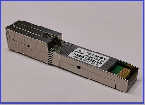
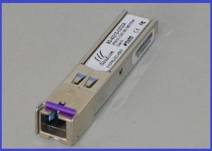
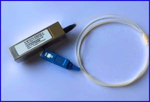
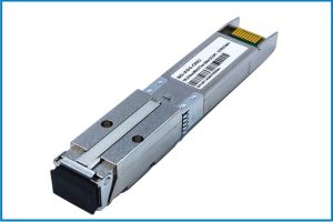
INFORMATION
Features
u Single fiber bi-directional
data links asymmetric TX 2500Mbps/RX1250Mbps application
u 1490nm continuous-mode DFB
laser transmitter and 1310nm burst-mode APD-TIA receiver
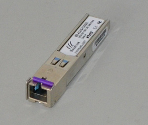
u Small Form Factor Pluggable
package with SC/UPC Connector
u Single 3.3V power supply
u Digital diagnostic
monitoring interface
u Low EMI and excellent ESD
protection
u RoHS6 Compliance
u LVPECL compatible data
input/output interface
u Class I laser safety
standard IEC-60825 compliant
u LVTTL fast receiver Signal
Detect (SD) indication response
u LVTTL transmitter disable
control and transmitter laser fault alarm
u Digital
burst RSSI function to monitor the input optical power level
Applications
u Gigabit Ethernet Passive
Optical Networks (GPON)
u Gigabit-Capable Passive
Optical Networks Class C+++ 60km 17~32dB attenuation range
Standards
u Complies with SFP
Multi-Source Agreement (MSA) SFF-8074i
u Complies with IEEE
802.3ah
u Complies with FCC 47 CFR
Part 15, Class B
u Complies with FDA 21 CFR
1040.10 and 1040.11 except for deviations pursuant to Laser Notice No. 50,
dated June 24, 2007
u Complies with SFF-8472
u Compatible with
TR-NWT-000870 4.1 ESD sensitivity classification Class2.
u Compatible
with Telcordia GR-468-CORE
Specification
|
Recommended Operating Conditions |
||||||
|
Parameter |
Symbol |
Min |
Typical |
Max |
Unit |
Notes |
|
Operating Case Temperature |
Tc |
-5 |
|
70 |
°C |
|
|
-40 |
|
85 |
|
|||
|
Power Supply Voltage |
VCC |
3.135 |
3.3 |
3.465 |
V |
|
|
Supply Current |
ICC |
|
|
500 |
mA |
|
|
Power Consumption |
PW |
|
|
1.65 |
W |
|
|
Data Rate |
|
|
2.5 |
|
Gbps |
|
|
Absolute Maximum Ratings |
||||
|
Parameter |
Symbol |
Min |
Max |
Unit |
|
Storage Ambient Temperature |
TSTG |
-40 |
85 |
°C |
|
Storage Humidity |
HS |
5 |
90 |
% |
|
Operating Humidity |
HO |
5 |
85 |
% |
|
Power Supply Voltage |
VCC |
0 |
+3.6 |
V |
|
Receiver Damaged Threshold |
|
+6 |
|
dBm |
|
Electrical Characteristics |
||||||
|
Parameter |
Symbol |
Min |
Typical |
Max |
Unit |
Notes |
|
Transmitter Differential Input Voltage |
|
300 |
|
2400 |
mV |
|
|
Receiver Differential Output Voltage |
|
500 |
|
1200 |
mV |
|
|
Transmit Fault Alarm Voltage |
VOH |
2.4 |
|
VCC+0.3 |
V |
LVTTL |
|
VOL |
0 |
|
0.4 |
V |
LVTTL |
|
|
Transmit |
VIH |
2 |
|
VCC+0.3 |
V |
LVTTL |
|
VIL |
0 |
|
0.8 |
V |
LVTTL |
|
|
Input |
|
90 |
100 |
110 |
Ω |
|
|
Transmit |
TOFF |
|
|
10 |
us |
|
|
Loss |
VOH |
2.4 |
|
VCC |
V |
LVTTL |
|
VOL |
0 |
|
0.4 |
V |
LVTTL |
|
|
Loss Of |
TD |
|
500 |
|
us |
|
|
Loss Of |
TA |
|
500 |
|
us |
|
|
Optical |
||||||
|
Parameter |
Symbol |
Min |
Typical |
Max |
Unit |
Notes |
|
Launched Power (avg.) |
POUT |
+7 |
|
+9 |
dBm |
C+++ |
|
+5 |
|
+7 |
C++ |
|||
|
+3 |
|
+5 |
C+ |
|||
|
Operating |
λC |
1480 |
1490 |
1500 |
nm |
|
|
Spectral |
∆λ |
|
|
1 |
nm |
|
|
Side Mode |
SMSR |
30 |
|
|
|
|
|
Extinction |
ER |
9 |
|
|
dB |
PRBS 27-1 |
|
Transmitter |
TDP |
|
|
2.3 |
dB |
Transmit on 80km |
|
Optical |
PDIS |
|
|
-32 |
dBm |
|
|
Output Eye Diagram |
Compliant |
|||||
|
Transmitter Reflectance |
|
|
|
-10 |
dB |
|
|
Optical |
||||||
|
Parameter |
Symbol |
Min |
Typical |
Max |
Unit |
Notes |
|
|
λC |
1260 |
1310 |
1360 |
nm |
|
|
Receiver |
SEN |
-29 |
|
-32 |
dBm |
Note1 |
|
Optical |
SAT |
-6 |
|
|
dBm |
Note1 |
|
LOS Assert Level |
LOSA |
-45 |
|
|
dBm |
|
|
LOS Deassert Level |
LOSD |
|
|
-31 |
dBm |
|
|
LOS Hysteresis |
HYS |
0.5 |
|
6 |
dB |
|
|
Receiver |
|
|
|
-12 |
dB |
|
Note 1: PRBS 27-1@1.25Gbps, transmitter is
operating, BER ≤1×10⁻¹⁰

Figure 1 RSSI TIMING SEQUENCE
|
RSSI Characteristics |
||||||
|
Parameter |
Symbol |
Min. |
Typ. |
Max. |
Unit |
Notes |
|
RSSI |
|
0 |
|
0.8 |
V |
|
|
RSSI |
|
2.0 |
|
Vcc |
V |
|
|
RSSI |
TD |
0 |
|
3000 |
ns |
|
|
Optical |
TONT |
300 |
|
|
ns |
|
|
RSSI |
TW |
300 |
|
TONT – |
ns |
|
|
I |
Tp |
|
|
500 |
μs |
|
Digital Diagnostic Monitoring Information
|
Parameter |
Accuracy |
Calibration |
Note |
|
Temperature |
±3°C |
External |
|
|
Voltage |
±3% |
External |
|
|
Bias Current |
±10% |
External |
|
|
TX Power |
±3dB |
External |
|
|
RX Power |
±3dB |
External |
|
Note: The digital
diagnostic monitoring interface defines 256-byte memory map in EEPROM, which
makes use of the 8 bit address 1010001X (A2h). Please refer to the SFF-8472 Rev
10.2 for the detail information.
Pin
definition
|
Pin |
Name |
Level/Logic |
Function |
Description |
|
1 |
NC |
NA |
NA |
Not |
|
2 |
TX_Fault |
LVTTL |
TX |
Fault |
|
3 |
TX_Dis |
LVTTL |
Transmitter |
Enable/Disable |
|
4 |
MOD-DEF2 |
LVTTL |
SDA |
I2C |
|
5 |
MOD-DEF1 |
LVTTL |
SCL |
I2C |
|
6 |
MOD-DEF0 |
MOD-DEF0 |
Module |
Definition |
|
7 |
Reset |
LVTTL |
Receiver |
Reset |
|
8 |
SD |
LVTTL |
Signal |
Detect |
|
9 |
RSSI |
Trigger |
RSSI |
High: enable RSSI A/D conversion |
|
10 |
GNDR |
NA |
Ground |
Receiver |
|
11 |
GNDR |
NA |
Ground |
Receiver |
|
12 |
RD- |
LVPECL |
RX |
Data- |
|
13 |
RD+ |
LVPECL |
RX |
Data+ |
|
14 |
GNDR |
NA |
Ground |
Receiver |
|
15 |
V |
cc |
R |
NA |
|
16 |
V |
cc |
T |
NA |
|
17 |
GNDT |
GNDT |
Ground |
Transmitter |
|
18 |
TD+ |
LVPECL |
TX |
Data+ |
|
19 |
TD- |
LVPECL |
TX |
Data- |
|
20 |
GNDT |
NA |
Ground |
Transmitter |
Typical application
Circuit

Figure
2 Typical Interface Circuit
EEPROM Memory Map

Figure
5 EEPROM Memory Map Specific Data Field Descriptions
EEPROM Serial ID
Memory Contents
The optical transceiver contains an EEPROM. It provides
access to sophisticated identification information that describes the transceiver’s
capabilities, standard interfaces, manufacturer, and other information. When
the serial protocol is activated, the host generates the serial clock signal
(SCL, Mod Def 1). The positive edge clocks data into those segments of the
EEPROM that are not writing protected within the SFP transceiver. The negative
edge clocks data from the SFP transceiver. The serial data signal (SDA, Mod Def
2) is bi-directional for serial data transfer. The host uses SDA in conjunction
with SCL to mark the start and end of serial protocol activation. The memories
are organized as a series of 8-bit data words that can be addressed
individually or sequentially.
The Module provides diagnostic information about the
present operating conditions. The transceiver generates this diagnostic data by
digitization of internal analog signals. Calibration and alarm/warning
threshold data is written during device manufacture. Received power monitoring,
transmitted power monitoring, bias current monitoring, supply voltage
monitoring and temperature monitoring all are implemented. The diagnostic data
are raw A/D values and must be converted to real world units using calibration
constants stored in EEPROM locations 56 – 95 at wire serial bus address A2h.
The digital diagnostic memory map specific data fields define as following.
EEPROM Serial ID
Memory Contents (2-Wire Address A0h)
|
Address |
Name of field |
Hex |
Description |
|
BASE ID Fields |
|||
|
00 |
Identifier |
03 |
SFP transceiver |
|
01 |
Ext. Identifier |
04 |
Serial ID module supported for SFP |
|
02 |
Connector |
01 |
SC |
|
03-05 |
00 00 00 |
Not defined |
|
|
06 |
Transceiver Codes |
80 |
BASE-PX |
|
07-10 |
Transceiver Codes |
00 00 00 |
Not defined |
|
11 |
Encoding |
01 |
8B10B |
|
12 |
BR, Nominal |
0C |
|
|
13 |
Rate Identifier |
00 |
Not defined |
|
14 |
Length(9um)-km |
14 |
20(km) |
|
15 |
Length(9um)-m |
C8 |
200(100m) |
|
16 |
00 |
Transceiver transmit distance |
|
|
17 |
Length(62.5um) |
00 |
|
|
18 |
Length(cable) |
00 |
Not support cable |
|
19 |
Length(OM3) |
00 |
Not support OM3 |
|
20-35 |
Vendor Name |
xx xx …. xx |
|
|
36 |
Reserved |
00 |
Not defined |
|
37-39 |
Vendor OUI |
00 00 00 |
Not defined |
|
40-55 |
Vendor P/N |
47 54 53 2D 53 45 54 31 31 2D 32 30 44 43(49) |
GPON-OLT-C+++”(ASCII character) |
|
56-59 |
Vendor P/N Rev. |
41 30 20 20 |
“A0”(ASCII character) |
|
60-61 |
Laser Wavelength |
05 D2 |
1490nm |
|
62 |
Reserved |
00 |
Not defined |
|
63 |
CC_BASE |
xx |
Check sum of bytes 0-62 |
|
Extended ID Fields |
|||
|
64-65 |
Options |
00 1A |
TX_Disable、TX_Fault and RX_LOS are implemented |
|
66 |
BR,max |
00 |
Upper bit rate margin,20% |
|
67 |
BR,min |
00 |
Lower bit rate margin,20% |
|
68-83 |
Vendor SN |
xx…..xx |
Vendor Serial Number in ASCII character |
|
84-91 |
Date Code |
Data Code |
Vendor Date Code in ASCII character |
|
92 |
Diagnostic Monitoring Type |
58 |
Digital Diagnostic monitoring implemented “External calibrated ” is implemented, |
|
93 |
Enhanced options |
E0 |
Optional Alarm/warning flags, soft Tx_Disable |
|
94 |
SFF-8472 compliant |
03 |
SFF-8472 compliant with revision 10.2 |
|
95 |
CC-EXT |
xx |
Check sum of bytes 64-94 |
|
Vendor Specific ID Field |
|||
|
96-127 |
Vendor Specific |
00 |
Vendor specific EEPROM |
|
128-255 |
Reserved |
00 |
Reserved for future use |
Package Outline

(unit:mm)
Related Products

Send an Inquiry
Tell us your required quantity, destination country, and any technical requirements. We'll reply within 12 hours.